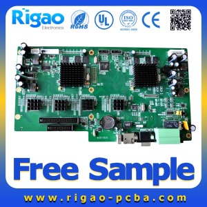
Rigao Electronics Co, . Ltd is an experienced PCB and PCBA manufacturer in Shenzhen, China. We are focus on manufacturing Printed Circuit Boards(PCB) and PCB Assembly(PCBA). OEM PCBA, SMT, DIP and final Assembly is our strengths.
After several years' developing and improving, our company establishes our main business in three principal areas-Printed Circuit Boards, PCB Assembly and Components Procurement. From prototype to mass production, we are able to gurantee a complete service with technical back up, offering a cost advantage and continuity of supply.
For making PCB Assembly(PCBA), customer just need to provide us with Gerber file and bill of material. Components procurement is one of the featured service we can provide. IC, battery, fuse, LCD, transformer, LED Diode, connector, sensor, we could purchase all these electronic parts to our customers.
Our aim: High quality, low cost & fast delivery for PCB and PCB Assembly.
Verification: UL, ISO9001: 2000, RoHS
Our PCBA capability and services: SMT/THT/DIP.
1. Component Purchasing Service
2. SMT assembly and Through hole components insertion
3. IC pre-programming / Burning on-line
4. Function testing as requested
5. Complete Unit assembly (which including plastics, metal box, Coil, cable inside etc)
6. Packing design
PCB/PCBA Description:
1. Singlesided PCB, double side PCB & multilayer PCB with competitive price, good quality and excellent service.
2. FR-4, FR-4 High TG, CEM-1, CEM-3, Aluminum base material.
3. HAL, HAL lead free, Immersion Gold/ Silver/Tin, OSP surface treatment.
4. Printed Circuit Boards are 94V0 compliant, and adhere to IPC610 Class 2 international PCB standard.
5. Quantities range from prototype to medium and batch production.
PCB/PCBA Features:
Dimension: 92.5mm*36mm
Base Material: 0.1mm Cu/25um ADH/25um PI+25um ADH/35um Cu/
20um ADH/ 35um Cu/ 2525um PI+25um ADH/
25um ADH/ 0.1mm Au
Thickness: 1.6mm
Line Width/Space: 0.15mm/0.15mm
Surface Treatment: ENIG: Au: 0.03-0.09um, Ni: 2-6um
Minimum via diameter: 0.2mm
The smallest hole: 0.35mm.
| SMT |
Position accuracy: 20 um |
| Components size: 0.4×0.2mm(01005) _130×79mm,Flip-CHIP,QFP,BGA,POP |
| Max. component height:: 25mm |
| Max. PCB size: 680×500mm |
| Min. PCB size: no limited |
| PCB thickness: 0.3 to 7mm |
| Wave Solder |
Max. PCB width: 450mm |
| Min. PCB width: no limited |
| Component height: Top 120mm/Bot 15mm |
| Sweat-Solder |
Metal type : part, whole, inlay, sidestep |
| Metal material: Copper , Aluminum |
| Surface Finish: plating Au, plating sliver , plating Sn |
| Air bladder rate: less than20% |
| Supporting: |
Software burning and Function Testing |
| Testing |
X-RAY Inspection & AOI Test, ICT, Probe flying, burn-in, function test, temperature cycling |
| Lead Time |
12days-15days |
| File Fomat |
Bill of Materials,Gerber Files, Pick-N-Place File (XYRS),PCB,Altium, EDA etc |

 Company Profile